Design and completion of new MBE machine

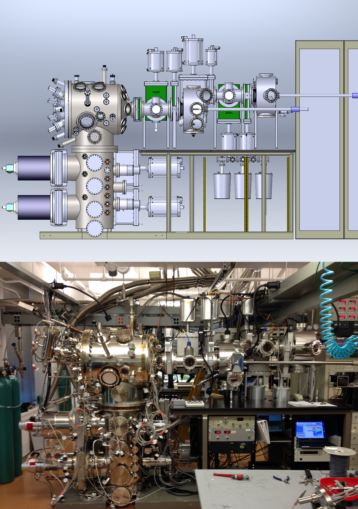
We designed and recently completed a new gallium arsenide (GaAs) MBE machine that has a uniquely-clean base vacuum. We developed a novel vacuum cryo-pump system that uses three massive cryo-coolers to cool several nickel-coated surfaces to 17K. These 17K surfaces are internal to the vacuum sump and growth environment of the new machine. Because of this internal geometry, the pumping speed of these cryo-surfaces is greatly enhanced compared to externally mounted pumps. When these internal cryo-surfaces are cooled to 17K, the vapor pressures of the dominant impurity gases, N2, CO, CH4, O2, and CO2, are each well below 10-12 Torr, and the base vacuum pressure in the MBE is lowered by an additional factor of 5 compared to pumping with only the externally mounted cryo-pumps. Altogether using both the internal and external cryo-pumping systems, the vacuum environment in the new MBE is more than an order of magnitude cleaner than any other MBE chamber. We are now exploring the impact of this improved vacuum environment on the quality of the 2D electron systems that they produce.
Mapping out 2D density variations

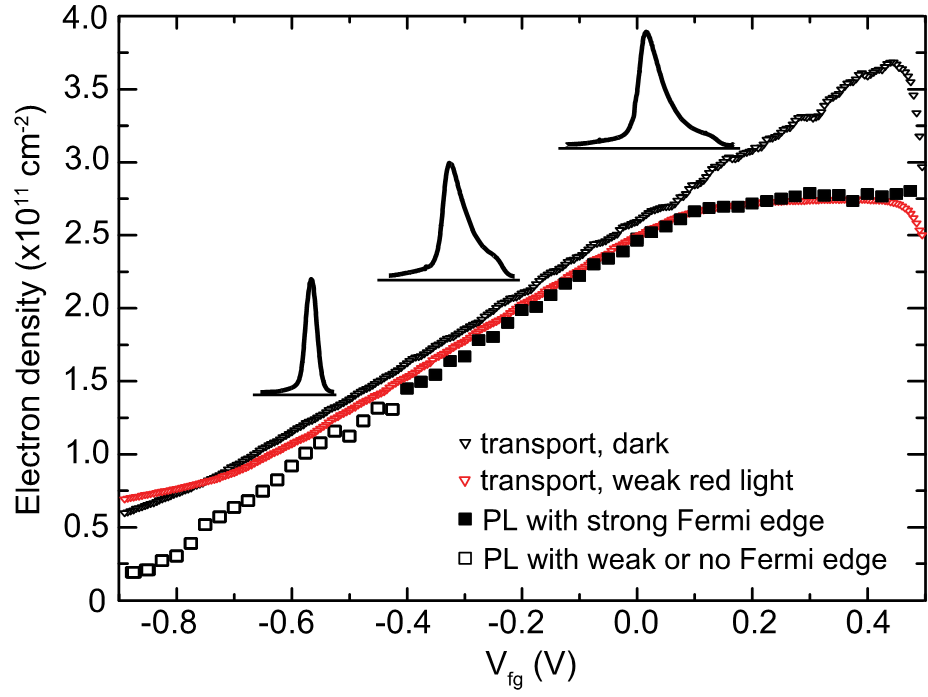
We compare micro-photoluminescence (PL) as a measure of the electron density in a clean, two-dimensional (2D) system confined in a GaAs quantum well (QW) to the standard magneto-transport technique. Our study explores the PL shape evolution across a number of MBE-grown samples with different QWs widths and 2D electron densities, and notes its correspondence with the density obtained in magneto-transport measurements on these samples. The main features of the PL spectrum and their relation with the 2DEG carrier density are summarized in the figure. The laser light creates electron-hole pairs which in turn induce recombinations between the 2D electron states in the QW, residing in the lowest n=1 energy level of the conduction band, and hole states created by the laser absorption in the valence band. These recombinations preserve momentum and appear as vertical transitions on the momentum diagram. The QW PL spectrum has a characteristic shape with a strong maximum near the bottom of the QW band and a Fermi-like shape. Both points can easily be determined from the derivative of the PL spectrum. Taking into account the Burstein-Moss shift, the Fermi energy can be calculated from the difference between the PL onset and the PL peak, thus providing a direct measurement of the 2DEG carrier density from the PL spectrum.

We also measure the 2D density in a top-gated quantum well sample using both PL and transport and find that the two techniques agree to within a few percent over a wide range of gate voltages. We find that the PL measurements are sensitive to gate-induced 2D density changes on the order of 109 electrons/cm2. The spatial resolution of the PL density measurement in our experiments is 40 microns, which is already substantially better than would be possible in spatial density mapping using magneto-transport. Our results establish that micro PL can be used as a reliable high spatial resolution technique for future contactless measurements of density variations in a 2D electron system.
Design rules for growing AlAs quantum wells
The fractional quantum Hall effect observed in clean 2D electron systems (2DES) is a remarkable consequence of electron-electron interaction. While GaAs has been the primary material of choice to examine such phenomena, AlAs has also proven to be an intriguing option as it differentiates itself from GaAs in its Landé g-factor, effective mass, valley degeneracy, and anisotropy in band structure. Studies have indeed reported the existence of valley susceptibility, valley Skyrmions, quantum Hall ferromagnetism, and anisotropy transference to composite fermions in AlAs 2DES. However, despite the abundant literature on AlAs 2DES, a systematic sample design is still unexplored for AlAs quantum well (QW) structures. Most of the studies on AlAs 2DES use an AlxGa1-xAs barrier alloy fraction x ? 40%. Although this is the Al alloy fraction at which we expect maximum carrier density in a modulation doped AlAs QW, it may not be the point of highest sample quality, as is well known in GaAs QWs where interface quality and unwanted impurities in the AlxGa1-xAs also play important roles. Our goal is to grow AlAs QWs with various barrier alloy fractions and evaluate their electrical properties to provide a guideline for sample optimization in AlAs 2DES.

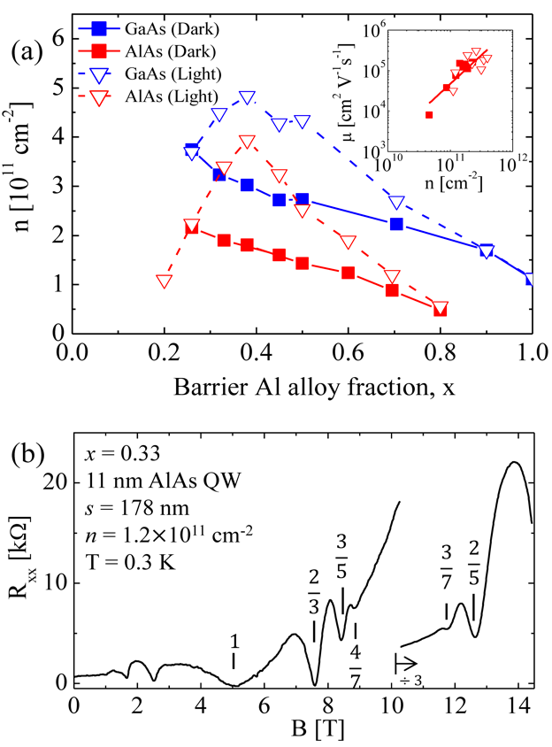
Figure 1(a) shows the measured carrier densities in modulation-doped AlAs QWs over the barrier alloy fraction range of 0.2 < x < 0.8, both in the dark and after light illumination. The spacer thickness (s) and well width (w) are 59 nm and 11 nm. Results are also shown for a series of GaAs QWs with s = 70 nm and w = 20 nm. From this data we can deduce all relevant energy levels for the modulation doping of the AlAs and GaAs QWs, and we find that there is good agreement between their values if we take the energy difference between the conduction band of GaAs(?) and AlAs(X) to be 114 meV. Once these values are established for all barrier alloy fractions, we can grow QWs with any density by varying the spacer thickness accordingly. Figure 1(a) implies that AlAs QWs with x < 0.38 barriers will behave similarly to GaAs QWs with x < 0.38 barriers. This hints that we can achieve high quality AlAs 2DES by using an AlxGa1-xAs barrier in this range. An example of a magneto-transport trace taken in such a sample is given in Fig. 1 (b). Even at the low density of 1.2×1011 cm-2, fractional quantum Hall states at fillings ν = 2/3, 3/5, 4/7, 3/7, and 2/5 can clearly be seen, indicating the high quality of the sample. These results provide a basis to investigate quality improvement in AlAs 2DESs, which is essential if we are to more carefully study the physics of electrons in this system.